martymcfly
Well-known member
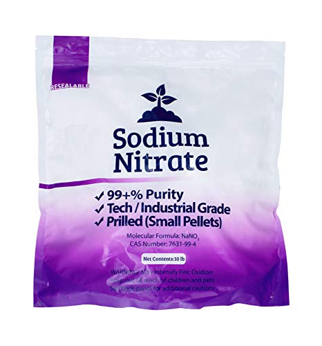
Currently im going to try to put 12 black fibre amds through A/R. I beleive these can be done the same way as ceramic processors using A/R @ 4 parts HCL to 1 part HN03 and using the calculation that 3.8ml of HCL + .95ml HN03 dissolves 1g of gold how do i work out how much i should use for my processors? my total weight is 150g with lids removed but obviously this is not all gold as i have fibre and kovar i think.
So would you recommend doing my calculation for this total weight of 150g or just cover processors with HCL and then add HN03 in drops of 3ml at a time untill reaction stops?
i feel that covering them completely and then just adding drops of nitric will do the job but would be grateful if someone with more experience can tell me if this is the best way to go about it?
My second question is, can i just sit them in HCL to dissolve what solder is left on them and then stick them to A/R or just go straight to A/R?
thanks
")