


- Joined
- Jun 22, 2023
- Messages
- 115
Since this question comes up all the time, I figured I could lend some insight. I've worked in the semiconductor industry for 20+ years for the companies that make these devices, so I have some insider knowledge and can debunk some myths as well.
So let's start off with this. Note that I am EXCLUDING Pentiums, enough has been done on those.

Sorry my chicken scratch is hard to read, but this is a good snapshot of the "majority" of IC packages you will find. Not all, but the common ones.
Top to bottom:
CERDIPs - CERAMIC Dual In Line Package - Some of mine are the Gold heavy test chips - average weight is 5G with 0.5G recoverable gold per device. These are hard to find but are, well, a gold mine. Especially with the "lid" these will produce a nice clean gold solution in AR. The gold ones are pretty easy to spot, but there are Tin leaded versions as well. Most if not all of the ceramic ones are gold bond wires, but you have to get to it. I personally think that CERDIPS are the easy to work with - just torch them, crush them, wash them, then into the AR. They do produce dark AR so you need to clean it a bit, but nothing gets stuck togethor.
Second is a PDIP - Plastic dual inline package - they come in all sorts of pin counts and sizes, but will only have pins on 2 long sides. PRE-2014 these are QUARENTEED to have gold bond wires. If you come across large batches of the same device, you can usually go to the manufacturer website and find the date codes. Starting in 2014, despite what others will say, the INDUSTRY as a WHOLE started switching over to hybrid bond wires, usually Cu, CuPd, or aluminum. Yes, there are still some outlier devices, but it's starting to be close to a 70/30 split of Cu vs Gold. It's just the truth, and there are plenty of documents from manufactures stating such. In fact, if you have a specific part number, the datasheet will tell you what the bond wires are. If it is aerospace, automotive or custom, it's 99% chance to be gold, but if it's a commercial device, more than likely Cu or CuPd (Again after about 2014)
PDIPS are OK and can yield, but it's a messy, long process of grinding, washing, washing again, grinding some more, then going through chemical processing. Plenty of videos out there.

You can see the difference is pretty clear what gold yield differences would be!
Next down are TQFP - "Thin Quad Flat Pack" - there are also SSOP and QFP's where an SSOP is a plastic package with leads on 2 sizes, versus QFP with 4. These are the majority of new plastic packages with small legs on all 4 sides. (called gull wing or J-lead )
Same as the PDIP, pre 2014 are guaranteed to be gold bond wires, post 2014 could be a mix. The leads are usually Tin over Copper, sometimes Silver over Tin, sometimes what they call "matte Sn" which is just, well, Tin. These are all considered "leaded packages" (you can see the little gull wings sticking up if you zoom in) and some have heatsinks on the bottom, usually aluminum. But again, these will all contain some sort of bond wire. BEWARE that High power devices are generally going to be aluminum or copper bond wires. RF devices more likely to be gold.
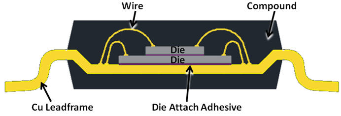

Next up are the dreaded BGA type packages. If you look careful you will see BGA's, and then on the (well, top since the picture is rotated) what is called a WLCSP - Wafer Level Chip Scale Package.
WLCSP's DO NOT HAVE BOND WIRES. PERIOD. The die is flipped upside down, solder balls are attached, and it's encapsulated in epoxy.
BGA's May have bond wires, or they may have a substrate (teeny tiny PCB inside the package, and the die is basically solder bumped and attached to that so it fans out the grid array). Only way to tell is grind a few up and process them with AR.
On an interesting note here - BGA's are the grandkids of the highly sought after PGA's - Pin Grid Array - found in the old pentiums and such that had sockets. If you look at a PGA it has a similar layout on the bottom to the BGA, just with solder bumps replacing the pins.
Here's the inside of a BGA - again may or may not have bond wires.

BGA solder balls are usually SnPd or SnCu - but OLD ones from the 80's and early 90's may be Silver or Gold - but watch out, a lot of those old parts also contain LEAD in the solder. (RoHS changed all of that in circa 2005)
Last on this list at least, are QFN's - Quad Flat No Leads - these will look like a TQFP or QFP, but there are no "legs" sticking out around the package. Rather they are flat solder pads incorporated into the edge of the plastic package.
These WILL have Bond Wires, but again no guarantee on gold, Cu or CuPd

In my opinion only, I prefer working with the ceramic packages
For additional reading, here's some documents from around the industry about bond wires.
Texas Instruments - Converting to Cu - https://www.ti.com/lit/wp/sszy003/sszy003.pdf?ts=1692081118893
Renesas Product Change Notification stating switch from gold to copper - https://www.renesas.com/us/en/docum...cility-listed-renesas-tssop-packaged-products
Renesas Copper bond wire overview - https://www.renesas.com/us/en/docum...stimating-bond-wire-current-carrying-capacity
Microchip some of their process nodes to CuPdAu (still some gold, but another alloy) https://www.microchip.com/product-c...8BVJU876/PCN_JAON-08BVJU876_Affected_ CPN.pdf
Hope this helps. I'm happy to keep adding more details if there are any requests!
So let's start off with this. Note that I am EXCLUDING Pentiums, enough has been done on those.
Sorry my chicken scratch is hard to read, but this is a good snapshot of the "majority" of IC packages you will find. Not all, but the common ones.
Top to bottom:
CERDIPs - CERAMIC Dual In Line Package - Some of mine are the Gold heavy test chips - average weight is 5G with 0.5G recoverable gold per device. These are hard to find but are, well, a gold mine. Especially with the "lid" these will produce a nice clean gold solution in AR. The gold ones are pretty easy to spot, but there are Tin leaded versions as well. Most if not all of the ceramic ones are gold bond wires, but you have to get to it. I personally think that CERDIPS are the easy to work with - just torch them, crush them, wash them, then into the AR. They do produce dark AR so you need to clean it a bit, but nothing gets stuck togethor.
Second is a PDIP - Plastic dual inline package - they come in all sorts of pin counts and sizes, but will only have pins on 2 long sides. PRE-2014 these are QUARENTEED to have gold bond wires. If you come across large batches of the same device, you can usually go to the manufacturer website and find the date codes. Starting in 2014, despite what others will say, the INDUSTRY as a WHOLE started switching over to hybrid bond wires, usually Cu, CuPd, or aluminum. Yes, there are still some outlier devices, but it's starting to be close to a 70/30 split of Cu vs Gold. It's just the truth, and there are plenty of documents from manufactures stating such. In fact, if you have a specific part number, the datasheet will tell you what the bond wires are. If it is aerospace, automotive or custom, it's 99% chance to be gold, but if it's a commercial device, more than likely Cu or CuPd (Again after about 2014)
PDIPS are OK and can yield, but it's a messy, long process of grinding, washing, washing again, grinding some more, then going through chemical processing. Plenty of videos out there.
You can see the difference is pretty clear what gold yield differences would be!
Next down are TQFP - "Thin Quad Flat Pack" - there are also SSOP and QFP's where an SSOP is a plastic package with leads on 2 sizes, versus QFP with 4. These are the majority of new plastic packages with small legs on all 4 sides. (called gull wing or J-lead )
Same as the PDIP, pre 2014 are guaranteed to be gold bond wires, post 2014 could be a mix. The leads are usually Tin over Copper, sometimes Silver over Tin, sometimes what they call "matte Sn" which is just, well, Tin. These are all considered "leaded packages" (you can see the little gull wings sticking up if you zoom in) and some have heatsinks on the bottom, usually aluminum. But again, these will all contain some sort of bond wire. BEWARE that High power devices are generally going to be aluminum or copper bond wires. RF devices more likely to be gold.
Next up are the dreaded BGA type packages. If you look careful you will see BGA's, and then on the (well, top since the picture is rotated) what is called a WLCSP - Wafer Level Chip Scale Package.
WLCSP's DO NOT HAVE BOND WIRES. PERIOD. The die is flipped upside down, solder balls are attached, and it's encapsulated in epoxy.
BGA's May have bond wires, or they may have a substrate (teeny tiny PCB inside the package, and the die is basically solder bumped and attached to that so it fans out the grid array). Only way to tell is grind a few up and process them with AR.
On an interesting note here - BGA's are the grandkids of the highly sought after PGA's - Pin Grid Array - found in the old pentiums and such that had sockets. If you look at a PGA it has a similar layout on the bottom to the BGA, just with solder bumps replacing the pins.
Here's the inside of a BGA - again may or may not have bond wires.
BGA solder balls are usually SnPd or SnCu - but OLD ones from the 80's and early 90's may be Silver or Gold - but watch out, a lot of those old parts also contain LEAD in the solder. (RoHS changed all of that in circa 2005)
Last on this list at least, are QFN's - Quad Flat No Leads - these will look like a TQFP or QFP, but there are no "legs" sticking out around the package. Rather they are flat solder pads incorporated into the edge of the plastic package.
These WILL have Bond Wires, but again no guarantee on gold, Cu or CuPd
In my opinion only, I prefer working with the ceramic packages
For additional reading, here's some documents from around the industry about bond wires.
Texas Instruments - Converting to Cu - https://www.ti.com/lit/wp/sszy003/sszy003.pdf?ts=1692081118893
Renesas Product Change Notification stating switch from gold to copper - https://www.renesas.com/us/en/docum...cility-listed-renesas-tssop-packaged-products
Renesas Copper bond wire overview - https://www.renesas.com/us/en/docum...stimating-bond-wire-current-carrying-capacity
Microchip some of their process nodes to CuPdAu (still some gold, but another alloy) https://www.microchip.com/product-c...8BVJU876/PCN_JAON-08BVJU876_Affected_ CPN.pdf
Hope this helps. I'm happy to keep adding more details if there are any requests!
") )
)