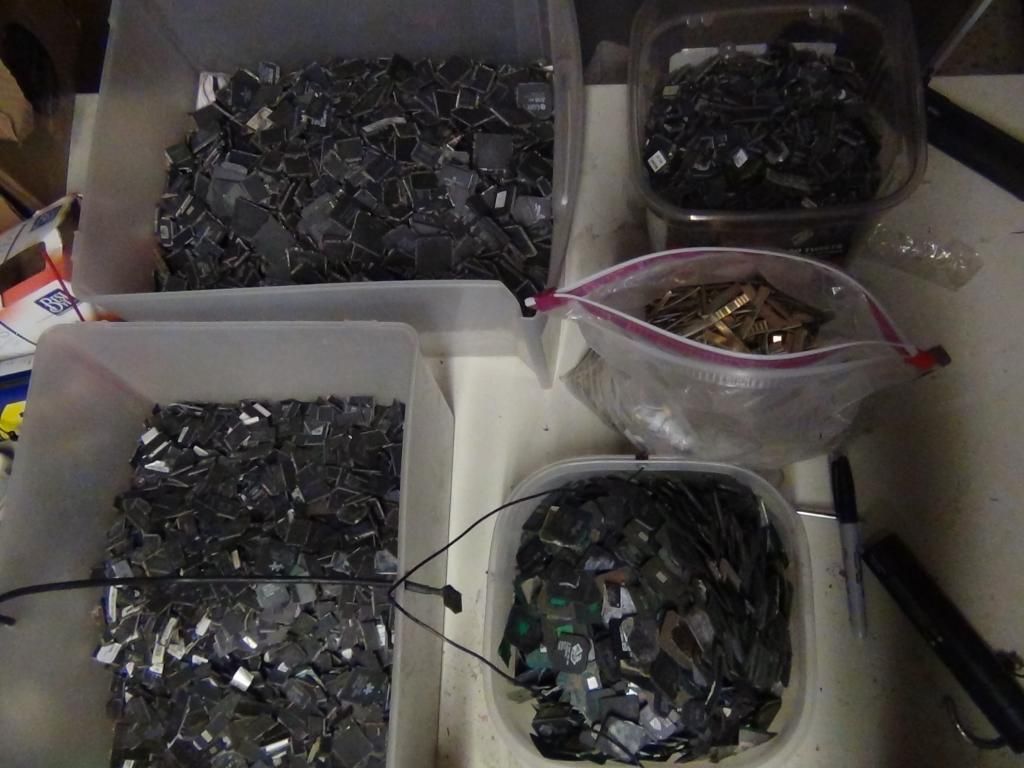
Gold inside chips (black, flatpacks - not CPU)

Gold Refining Forum

Help Support Gold Refining Forum:

This site may earn a commission from merchant affiliate links, including eBay, Amazon, and others.
And if you need manuals they are here: http://bitsavers.trailing-edge.com/pdf/ibm/system36/

I've been looking for one of those for a couple of years now but so far none have surfaced here in northern Sweden.
But in two weeks time I'm picking up a Datapoint 2200, more than a decade older than IBM system 36.
The memory in the DP-2200 is round metal capsules with 512 bits per capsule. Fully expanded it has 8 kbyte! :mrgreen:

Göran
 
s/n bridge chips you should avoid.

From now on I am separating s/n to 2 types. Computer and video cards do have s/n on which bottom green part is thin, we all know how it look like.
There are different s/n which can be found on boards from TV. Those do have green part which feel considerably thicker, I would estimate double of computer s/n. They also have round shaped metallic heat sink visible on black top part. When incinerated some of them do have big square metal piece, I did not identify what metal it is but it is soft. I recently processed 1.7 kilogram of them which is 3.74 pounds and yield was 2.6 gram of gold. So this is very important message to everyone who purchase s/n always check source or do visual/touch check - green bottom part must be thin for better variety which yield 5g+/kg and if thicker and with visible metallic heat sink part then yield is just 1.5g/kg.
The ones I processed did have Vise View logo.

*edited added pictures
 

Attachments

  • DSC_0038.jpg
    DSC_0038.jpg
    122 KB
  • DSC_0042.jpg
    DSC_0042.jpg
    88.6 KB
the copper heat spreader and then theres an aluminum piece that is shaped somewhat like a star (these differ from each other too).they break into pieces that looks like fluffy white metal that does not react to nitric acid. you can add hcl first until all the fizzing stops and then dry and incinerate the material. the nitric bath will then remove the copper legs with no problems.
 
Greetings Everyone!

Awesome Thread (old school, I mean topic). Sorry I'm new and should probably keep my mouth shut and just keep reading. It took me 2 days to read all of this and my head is spinning. I'm not yet prepared knowledge wise or equipment wise to attempt this, but it is what I was seeking to learn when I found your forum. I did skip over a bit but only after learning one of the most important things spoke of here. The danger in trying something that a group of experienced people won't consider because of safety concerns. Thank you for that.

The thing I was wondering about has been touched upon near the end. Older chips and a while back newer chips. I read that after 1998 there began a movement away from gold (ie gold bonding wires) and some newer processors have no gold whatsoever in them. The same article mentioned that older ic's and transistors used more gold (thicker wire). patnor seems to have dispelled the older chip theory I was forming. I'm going to keep collecting and reading for now.

Thank you patnor and the many others here for giving me a wealth of knowledge. If I may borrow from a couple of the signatures here: Knowledge is Power, but Experience is wisdom... both can help clear ignorance ...stupid is still incurable. I hope I'm just ignorant ;)
 
bonding technology started out using different types of metal for connecting the base to the die. the two main types are aluminum and gold. these two metals were used from the beginning and both metals were used even in the same type of processor chip. trying to determine which chips contain gold bonding wires by outside appearance is next to impossible.
 
Hi Pat! Still going strong here. I did a little organizing and took a picture. Starting at the top left going clockwise, 2880g memory stick chips and similar looking ones ( thin with tiny legs), 3240g miscellaneous tiny ic's with big legs, 4lbs gold fingers of wide variety from old to not so old, 5440g medium ic's with many tiny legs, 1720g s/n ic's.

Taking it one slow step at a time. Absolutely no hurry here. I've got some more goodies coming down the pike again too. Some telecom cabinets and some school networking equipment. :D

Anybody want to take a stab at an estimated yield for this?

Awesome stuff, I'm having more fun than should be allowed! :)

 
There is a very valuable list of tested yield on those here on the forum, I just can't find the link:

Testing Black Chips and SMD Packages on their Raw
Gold Content.pdf
 
I would say more. 8)
Notice that his s/n are just black top. Whole pieces yield 5+g/kg yet when we talk about black top part that could and should run about double of that. I would say that he should get 13+g just from his s/n.
I would estimate close to ounce there.
 
I'm sorry Pat, the whole sn parts are there I just hastily lumped them together for a picture so that's good news thanks! I actually have quite a bit more to harvest still. That's interesting about the TV s/n chip because I've got quite a bit of tv scrap here and the local scrap guy has a lot too. Will have to take a second look and thanks for the input Solar!
 
Geo said:
bonding technology started out using different types of metal for connecting the base to the die. the two main types are aluminum and gold. these two metals were used from the beginning and both metals were used even in the same type of processor chip. trying to determine which chips contain gold bonding wires by outside appearance is next to impossible.

I've been dabbling in the electronics industry for about 40 years now and my understanding is the only two metals used for bonding is gold and aluminum. There may be some weird high temperature aerospace application where platinum is used but I'd expect that to be rare. Aluminum bond wire is used in cheaper electronics like VCRs, older TVs, radios and stereos... you know, the junk that comes from China. It has a lower reliability because of the die bonding used but for the most part it works ok.... :lol: at least until the warranty expires.

Applications that demand more reliability (computers) will see gold bond wires attached to the die.

The thing is, you can't tell one from the other because of the black epoxy so you might as well incinerate and process all of them.
 
solar_plasma

This thought is directed your way since you have panning trouble with the flatpacks.

Think wind for a moment.
A long white sheet of paper in front of a slow blowing fan.
Black incinerated powder slowly dropped in the wind path and allowed to slightly be blown along untill it hits the paper.

Gold being heavier, would it not be closer to the fan then alot of the other dust?

The idea being to concentrate gold and bigger pieces needing further crushing, seperation.

In my odd mind, it would rid most of the black powder as it moves further along with the wind from a fan.

To test, I will someday crush my pyrolized packs and empty the garage floor and start with a gentle breeze and look with the magnifying glass down the paper to see if it works, or just causes me to sanitize the garage.
When I empty the garage of course....I think there is a floor there somewhere.

B.S.
Idea? or no?
 
i think water would be a better medium in any use of separating ash from the bonding wires. the wires, being wires, are going to be more aerodynamic than the really fine dust.
 

Latest posts

Back
Top